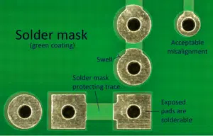
Solder mask, sometimes also referred to as solder stop mask or solder resist, is a thin layer of polymer that is usually applied to the copper traces of a printed circuit board (PCB). This layer of lacquer serves to protect against oxidation and to prevent short circuits from forming between the conductors that are close to each other. A short circuit is an unintended electrical connection between two conductors.
PCB manufacturers use solder mask to prevent this. Hand soldering operations do not require a solder mask coating, but for machine soldering (mass production), where the printed circuit board is automatically assembled and soldered using a wave soldering machine or in a reflow oven, solder mask is essential! Without a solder mask there would be one big short circuit (electrical short/solder bridge). After the PCB manufacturer has applied the solder mask, holes/openings must be made in the solder mask where components are soldered. This is achieved using photolithography. Solder mask is traditionally green, but is also available in many other colors.
Circuit board with green solder mask coating.
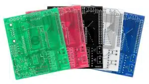
Solder mask coating in different colors.
Solder mask comes in different forms depending on the requirements and the application. The cheapest solder mask is an epoxy liquid that is screen printed through a pattern on the printed circuit board. Other types are the liquid photoprintable solder mask (LPSM or LPI) inks and dry film photoprintable solder mask (DFSM). LPSM can be screen printed or sprayed onto the circuit board, exposed to the pattern and designed to provide openings in the pattern for components to be soldered onto the copper pads. DFSM is vacuum laminated to the printed circuit board and then exposed and developed. All three processes typically undergo thermal curing of some type after the pattern is defined, although LPI solder masks are also available in ultraviolet (UV) curing.
In electronic design automation (EDA/ECAD), the solder mask is treated as a layer of the printed circuit board and is described as a Gerber file like any other layer, such as the copper and screen printing layers. Typical names for these layers are tStop/bStop (EAGLE), LSMVS/LSMRS (WEdirect) or GTS/GBS (Gerber and many others).
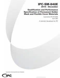 In the IPC-SM-840 “Qualification and Performance Specification of Permanent Solder Mask and Flexible Cover Materials” you will find much more information about the different solder mask materials, types, drying time, adhesion, moisture resistance, etc.
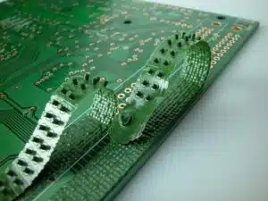
Example of peelable/temporary solder mask.
There is also a removable/temporary solder mask (peelable/temporary solder mask). This lacquer is used to provide temporary protection and is removed (teared off) after soldering.
The solder mask testing is done via the tape test or via the peeling test.
The hardness (after curing) is tested with a pencil.
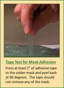
Example of tape test (with special adhesive tape).
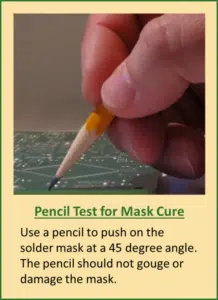
Pencil test example.
Further information on solder mask testing can be found in IPC-TM-650.