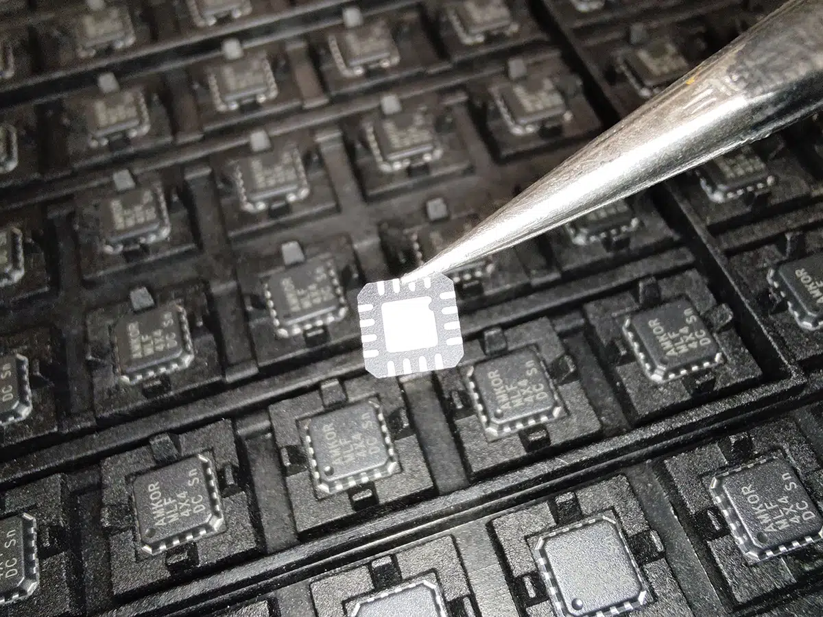
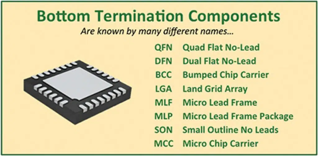
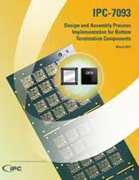
BTC-components are the “new generation” ICs that take up considerably less space than their “older” predecessors such as QFPs, SOICs, etc. BTCs (as the name suggests) do not have leads (legs) on the side of the component but metallized surfaces on the bottom (bottom terminations). This makes them faster, lighter and cheaper than their predecessors. Because they are so thin, they are very suitable for mobile phones and other consumer electronics. At the bottom, BTCs have a large cooling surface that excellently dissipates heat to the printed circuit board.
 However, there are also disadvantages when using these BTC components. The assembly process must be closely monitored. The right amount of solder paste is critical for a good solder joint. If too much solder paste is applied, the BTC component will “float” on the paste, which can cause a short circuit. If too little solder paste is applied, open solder joints (no contact), voids, etc. are created. An additional disadvantage is the inspection of BTC components. For this you need X-ray equipment. Due to the small opening (gap) under the component (stand-off), it is also more difficult to clean the flux residues, you just can’t reach it. Because BTC components have no leads (which can absorb any expansion forces/vibrations), the reliability of these components is only determined by the correct amount of solder. Due to the solvents inside the flux in the solder paste, you often have problems with voiding (holes) in the X-ray image below the thermal plane.
Special design and assembly process guidelines for BTC-components can be found in IPC-7093 “Design and Assembly Process Implementation for Bottom Termination Components”.
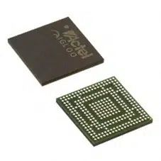
BGA-components (Ball Grid Arrays) have been available on the market for some time.
Based on the different packaging materials, BGA components can be classified into the following types: PBGA (plastic ball grid array), CBGA (ceramic ball grid array), CCGA (ceramic column grid array), TBGA (tape ball grid array) en CSP (chip-scale package).
The leading properties (advantages) of BGA components include:
A. Because there are no leads around the housing but solder balls (bumps) on the underside of the component, the pitch distance (the distance between the balls) is greater and more bumps/balls can be positioned on the same component size.
B. Higher component reliability, lower solder joint failure rate and higher solder joint reliability (stronger).
C. Alignment of QFPs (quad flat package) is usually achieved through visual observation by operators and these QFP components are difficult to align and solder. BGAs are “self-aligning” (due to the surface tension the component pulls itself into the correct position) and therefore easier to center. This self-alignment works even if the BGA component is up to 50% off set from the pads/lands.
D. It’s easy to print solder paste through a stencil onto BGA components.
E. BGA terminations (balls/colums) are stable with better flatness than QFP component, because the flatness error can be automatically compensated between the package body and PCB (printed circuit board) after solder ball melting.
F. Due to the excellent electrical properties, BGA components make it possible to reach very high frequencies.
G. BGA components perform better in terms of thermal dissipation (heat dissipation).
In addition to advantages, BGA components also have disadvantages. A major drawback is that it is difficult to inspect the quality of solder joints, which relies on AXI (automated X-ray inspection) and AOI (automated optical inspection) equipment capable of observing the melting of solder balls. Of course, the inspection costs and the level of difficulty also increase.
Storage and assembly environment of BGA components
PBGA components are moisture sensitive and thermal sensitive components, so they should be stored in a dry environment with constant temperature. Operators must be trained to comply with this technology process to prevent components from malfunctioning prior to assembly. In general, the optimum storage environment for BGA components is within the temperature range of 20°C to 25°C with a relative humidity of less than 10% RH. BGA components are best stored with nitrogen gas.
In general, when the MBB (moisture barrier bag) is once opened, the trays containing BGA components should never be exposed to air for long periods of time during the assembly and soldering process to avoid components absorb humidity leading to a reduction in solder quality due to low quality. Once MBBs (packaging) containing BGA components have been opened, they must be used up within 8 hours in an operating environment of ≤30°C/60% RH. When components are stored in nitrogen, the pot life can be extended to some extent.
It is very common to see that BGA components are not used up once the package (MBB) has been opened during SMT (surface mount technology) mounting. BGA components must be dried (tempered in a drying oven) next time before use to maintain their excellent solderability. The drying temperature (in the tempering oven) is usually around 125°C. The relationship between drying time and component thickness can be summarized in the table below.
Too high drying temperatures will lead to a change in the metallographic structure at the connection between solder balls on the component. Balls can become detached from the component housing, reducing SMT assembly quality. If the drying temperature is too low, no dehumidification (drying) will take place. Because the moisture in the component housing expands in the reflow process, the housing of the PBGA can crack, this is what they call the “popcorn” effect. BGA components can be reassembled after 30 minutes of drying and cooling in their natural assembly environment.
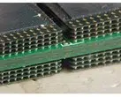 The future of the BGA is in the PoP components (Package-on-Package), where several BGA components are stacked on top of each other. They also sometimes call this “stack” packages (stacked components).
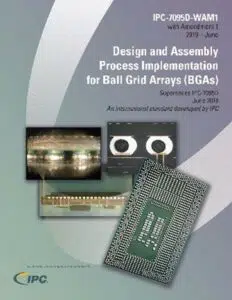 Special guidelines fort he design and assembly process for BGA-components and the latest trends can be found in IPC-7095 “Design and Assembly Process Implementation for Ball Grid Arrays (BGAs)”.

